


Advanced packaging is stretching semiconductor inspection in two directions at once: packages are getting larger while the features inside them are getting smaller.
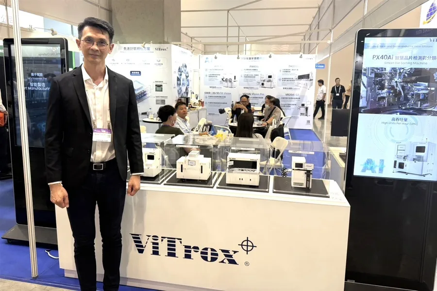
ViTrox sees chip inspection moving upstream as advanced packaging raises defect costs
DIGITIMES