Nature Communications, Published online: 13 June 2026; doi:10.1038/s41467-026-74218-2 Liang et al. present flexible semiconductive polyMOF membranes, created by copolymerizing metal–organic frameworks with polymers. This integration reduces structural defects and improves charge transport, enabling highly sensitive X-ray detection with leading sensitivity and a conformal design suited for flexibl…
A team of researchers from the Massachusetts Institute of Technology (MIT) and other institutions has developed a new way to improve the performance of powerful electronic devices by using an ultrathin layer of diamond. The breakthrough could help future technologies such as 6G wireless networks, satellite communications, radar systems, and even data centers operate faster […] The post Ultrathin …
Nature Communications, Published online: 12 June 2026; doi:10.1038/s41467-026-74341-0 Bi-based chalcogenides and oxychalcogenides host interesting topological, ferroelectric and optoelectronic properties, but a generable synthesis method of this material family is still missing. Here, the authors report the growth of mm-sized Bi-based chalcogenide and oxychalcogenide crystals on K+-free mica surf…
Funded by the European Commission and participating Member States under the Chips JU, FAMES continues to accelerate the early‑stage research shaping the next generation of FD‑SOI. The post CEA‑Leti Advances European FD-SOI Innovation with GlobalFoundries’ Collaboration in the FAMES Pilot Line appeared first on Semiconductor Digest .
With silicon semiconductors approaching their physical limits and data demands climbing, photonic integrated circuits offer faster, more energy-efficient data processing — though fully replacing electronic circuits remains a complex transition. The post Can Photonics Completely Replace Electronic Circuits? appeared first on Semiconductor Digest .
Energy-efficient thermal insulation is emerging as a small but critical process enhancement, cutting heat-transfer loss and helping fabs modernize without complete facility overhauls. The post The Unseen World of Semiconductor Insulation appeared first on Semiconductor Digest .
Silicone-based thermal interface materials (TIMs), particularly thermally conductive compounds and gels, offer material properties and performance characteristics that are well-suited to today’s data center applications. The post Silicone-Based Thermal Interface Materials Improve Data Center Cooling and Performance appeared first on Semiconductor Digest .
For decades, silicon has been the foundation of modern electronics because it is abundant, relatively affordable, and well suited to the precise control of electrical current that makes computer chips possible. But today’s most advanced systems, from AI hardware to high-power and quantum technologies, are pushing silicon harder than ever, demanding more speed, more power, … The post Great Lakes C…
Nature, Published online: 10 June 2026; doi:10.1038/s41586-026-10596-3 Efficient blue perovskite light-emitting diodes with an external quantum efficiency of 21.8% are achieved through in situ polymerization-driven nanocrystal confinement.
Moore's Law, the core driver of the semiconductor industry for over half a century, is now approaching its physical limits. The traditional path of solely shrinking transistor sizes has陷入 a triple dilemma of "slowing performance improvement, power consumption explosion, and soaring costs". The traditional chip paradigm, based on reductionist cognition, treats chips as linear collections of transi…
Second system order follows successful evaluation. The post Veeco Receives Follow-On Order for Nanosecond Annealing System appeared first on Semiconductor Digest .
Picosecond lasers with “burst-on-the-fly” pulsing can improve processing speed, via quality, and total cost-per-via for Ajinomoto Build-up Film (ABF) drilling. The post Optimizing ABF Drilling with Picosecond Lasers appeared first on Semiconductor Digest .
Nature Electronics, Published online: 09 June 2026; doi:10.1038/s41928-026-01658-5 Two-dimensional β-TeO 2 as an intrinsic insulator despite conflicting transport signatures
Nature Communications, Published online: 09 June 2026; doi:10.1038/s41467-026-74149-y The fabrication of p-type contacts for 2D semiconductors remains an important challenge towards the industrialization of 2D electronics. Here, the authors report a low-temperature molecular beam epitaxy contact strategy using a high-work-function Au1-xSex alloy to achieve Fermi-level depinning in monolayer WSe2 …
Scientists have developed a new way to manufacture ultra-thin semiconductors that could help power the next generation of computers, smartphones, and other electronic devices. Researchers led by Professor Cong Su have found a technique that combines high material quality with large-scale production, solving a long-standing challenge in semiconductor manufacturing. Their findings were published in…
Covalent today announced a strategic collaboration with Oxford Instruments that expands its semiconductor characterization offering with customer-ready, wafer-level Raman and photoluminescence (PL) workflows. The post Covalent Expands Wafer-Level Semiconductor Characterization Through Oxford Instruments Collaboration appeared first on Semiconductor Digest .
New LV100-type standard package with integrated 3-level circuit contributes to standardized inverter designs. The post Mitsubishi Electric and Semikron Danfoss Jointly Develop New Standard Package for Power Semiconductor Modules appeared first on Semiconductor Digest .
Researchers have demonstrated the ability to use van der Waals forces to tune the physical and electronic properties of ferroelectric thin films. The work opens the door to new techniques for engineering materials for use in smaller, more energy efficient electronic devices. The post Van der Waals Forces Can Play Unexpected Role in Thin Film Properties appeared first on Semiconductor Digest .
Nature Communications, Published online: 08 June 2026; doi:10.1038/s41467-026-74097-7 The behavior of metal-insulator transitions can be impacted by interaction and disorder mechanisms. Here, the authors identify metal-insulator transitions at carrier densities on the order of 1010 cm−2 in PtSe2 devices and evidence of a crossover in the metal-insulator transition behavior.
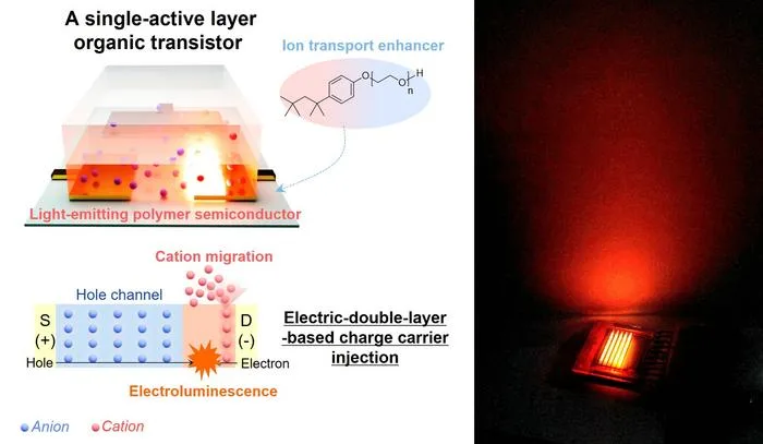
Koreans Fold Processing, Memory, and Light Into a Single Soft Transistor
When the transistor operates, a hole channel forms while a cation-induced electric double layer builds up at the drain electrode. This lets electrons and holes recombine to produce light. The effect depends on cations migrating on their own, driven by the ion-transport enhancer in the active layer. Because this double-layer …
materialsnanomaterialssemiconductors
research.io
Sign up to keep scrolling
Create your feed subscriptions, save articles, keep scrolling.