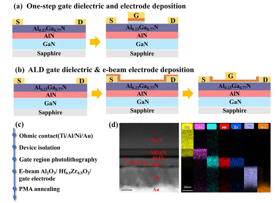
Scientific Reports, Published online: 11 May 2026; doi:10.1038/s41598-026-52482-y Structural, optical, and photodetection characteristics of thermally evaporated Azure A chloride/FTO thin films
Overview of the biaxial combinatorial sputtering approach and the resulting films. a Schematic of the combinatorial radio frequency (RF) magnetron sputtering scheme; b mapping of composition ratio across a 2-inch wafer; c cross-sectional SEM images at various positions in the sample.
The kSA XRF (X-Ray fluorescence) tool measures film thicknesses below 100 nanometers for applications in coated glass, solar panels, and more. The post k-Space Launches Its Newest Thin Film Metrology Solution appeared first on Semiconductor Digest .
This process is a two-stage atomic layer deposition (ALD) process that uses hydrogen film formation to create a thin anti-oxidation film and oxygen for the deposition of a high-quality ruthenium film. The post TANAKA Establishes New Ruthenium Film Deposition Process appeared first on Semiconductor Digest .
Despite the many advantages of laser ablation, typical PLD suffers from ejection of micro scale particulates (or droplets) during the target ablation process. The deposition of such particulates is usually undesired in many applications as they can deteriorate the electrical, chemical, optical, and mechanical properties of the film. It is possible to reduce the density […]